Failure Analysis
Our Wafer Metrology equipment offer unique stress/defect analysis and ion implantation monitoring for quality inspection of 300 mm wafers for high volume manufacturers.
SIRD: Scanning InfraRed Depolarization
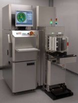
The SIRD is a stress measurement system at wafer level for process monitoring, which will contribute to cost reduction as well as yield improvement.
The introduction of the 300mm wafers has brought new standards for the suppliers of bare wafers: The increase to 300mm diameter has more than doubled the wafer surface area and weight; however, the thickness has remained very much the same, substantially increasing the risk of breakage. Whenever a 300mm wafer has areas of high internal mechanical tensions (stress), this will significantly increase the breakage probability during the IC manufacturing process along with all the implied very costly consequences. Therefore, the early detection of stressed wafers and prevention of breakage has gained more and more attention. Additionally, wafer stress does also have a negative influence on Silicon crystal lattice characteristics hence the device functionality.
TWIN: Thermal Wave Implant Dose Monitoring System
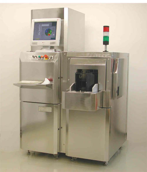
The Implant process is a very critical step within the integrated circuits manufacturing line. It defines important characteristics and properties of the devices-to-be by doping certain layers of the silicon substrate. Rework processes is very difficult and often impossible to apply. Hence, constant quality monitoring of the implant process is inevitable in order to maintain device yield. The TWIN system can measure on monitor as well as on product wafers. Its measurement range covers the entire range from 10E10 to 5E16 of dose level with an implant energy level from 1keV bis 100 MeV.